RF PCB stands for “radio frequency printed circuit board.” As their name suggests, RF PCBs function with high-frequency signals—typically within the radio frequency (RF) range, which can stretch from a few megahertz to several gigahertz. To keep these signals intact and free of interference, RF PCBs are made with specialized materials that minimize signal loss and distortion. They also feature controlled impedance and transmission line structures to maintain proper electrical conductivity.
In addition to ensuring signal integrity, RF PCBs must meet a number of other key design criteria to ensure reliable operation. For example, they need to be robust enough to resist the effects of electromagnetic interference and vibration, and they must be able to withstand higher operating temperatures than traditional PCBs. These requirements are essential to the reliability of RF PCBs, which are used in many applications including automobile anti-collision systems and satellite communication equipment.
The RF PCB is one of the fastest-growing sectors in PCB manufacturing, and it is important to understand the challenges associated with its development. When it comes to RF PCB assembly, there are a variety of issues that can arise from improper handling and layout. These issues can include signal degradation, solder joint failures, and delamination. Fortunately, these problems can be avoided with proper design and fabrication techniques.
To ensure the reliability of RF PCBs, manufacturers must adhere to a series of strict testing and inspection standards. These tests can include automated optical inspection and X-ray scanning to detect defects in the substrate, traces, and solder joints. They can also utilize network analysis to measure S-parameters and other important performance metrics. Additionally, RF PCBs can undergo thermal and electrical testing to ensure that they are capable of performing in the expected operating temperature range.
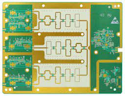
What Does RF PCB Stand For?
The future of RF PCBs is promising, as they provide the wireless connectivity and high-frequency circuitry that power cutting-edge applications across industries. For instance, 5G technology relies on RF PCBs to support high data rates and seamless connectivity across networks. Additionally, flexible RF PCBs are poised to revolutionize consumer electronics by enabling foldable displays and wearable health monitors.
Regardless of the application, the right rf pcb can improve functionality and reduce cost by enabling efficient wireless communications. To get the most out of your RF PCB, make sure to use advanced PCB design software that supports high-frequency designs, including circuit simulation, routing, and layer stack tools. Using these tools can help you create a design that meets your unique requirements while maintaining signal integrity.
A Radio Frequency (RF) Printed Circuit Board (PCB) is a specialized type of PCB designed to operate at high frequencies, typically ranging from MHz to several GHz. These boards are crucial in a wide array of applications, including wireless communications, radar systems, and satellite technology, where they facilitate the transmission and reception of RF signals.
One of the critical aspects of designing RF PCBs is the selection of materials. Common materials used include PTFE (Teflon), ceramic-filled laminates, and Rogers materials, which offer low dielectric constant and low loss tangent. These properties are essential for minimizing signal loss and ensuring signal integrity at high frequencies.