custom pcb be used in harsh environments
Custom PCBs (Printed Circuit Boards) have become indispensable in modern electronic systems, offering tailored solutions to meet the diverse needs of various industries. However, when it comes to harsh environments, where factors like extreme temperatures, high humidity, vibrations, and corrosive agents abound, the suitability of custom PCBs may come under scrutiny. In this article, we explore the potential and challenges of using custom PCBs in harsh environments.
The first consideration in deploying custom PCBs in harsh environments is the selection of appropriate materials. Traditional PCB materials like FR-4 (Flame Retardant 4) may not withstand the rigors of harsh conditions, leading to degradation, electrical failures, and shortened lifespan. Instead, specialized materials such as high-temperature laminates, metal-core PCBs, and ceramic substrates offer enhanced durability and reliability in harsh environments. These materials exhibit superior thermal conductivity, mechanical strength, and resistance to moisture, chemicals, and other environmental stressors.
Moreover, the design of custom pcb for harsh environments must prioritize robustness and resilience. Components should be carefully selected for their suitability to withstand extreme temperatures, humidity levels, and mechanical vibrations. Solder joints and connectors must be reinforced to withstand thermal cycling and mechanical stress, while conformal coatings and encapsulation can provide additional protection against moisture, dust, and corrosive agents.
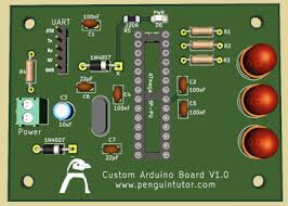
Can custom pcb be used in harsh environments?
Furthermore, the layout and routing of custom PCBs play a crucial role in ensuring reliability and performance in harsh environments. High-speed signal traces should be routed away from areas prone to electromagnetic interference (EMI), while power and ground traces should be designed to minimize impedance and voltage fluctuations. Additionally, adequate clearance and creepage distances should be maintained to prevent arcing and short circuits in high-voltage applications.
Another consideration in using custom PCBs in harsh environments is thermal management. Extreme temperatures can adversely affect the performance and reliability of electronic components, leading to thermal runaway, solder joint failure, and device malfunction. Custom PCBs can incorporate thermal vias, heat sinks, and other cooling mechanisms to dissipate heat effectively and maintain optimal operating temperatures in harsh environments.
Despite the challenges, the versatility and customization capabilities of custom PCBs make them well-suited for a wide range of harsh environment applications. Whether in aerospace, automotive, industrial, or military applications, custom PCBs can be tailored to meet the specific requirements and constraints of the environment, ensuring reliable operation under adverse conditions.
In aerospace and defense applications, for example, custom PCBs are used in avionics systems, missile guidance systems, and ruggedized communication equipment, where reliability and performance are paramount. Similarly, in automotive and industrial settings, custom PCBs find applications in engine control units (ECUs), powertrain systems, and harsh environment sensors, where they must withstand temperature extremes, mechanical shock, and vibration.
In conclusion, while deploying custom PCBs in harsh environments presents challenges related to material selection, design, and thermal management, careful consideration and implementation of best practices can overcome these hurdles. By leveraging specialized materials, robust design techniques, and advanced manufacturing processes, custom PCBs can deliver reliable performance and longevity in even the harshest of environments. As technology continues to advance and the demands of harsh environment applications evolve, custom PCBs will play an increasingly vital role in powering the next generation of electronic systems.