Electronics Circuit Boards Designed
Printed circuit boards are the key to all our electronic devices. They enable the signals and power to flow between all the different components and make our smartphones, computers, and heart rate monitors function properly. To do so, they contain conductive copper pathways that are used to conduct electricity between all the components.
These pathways are called nets and are outlined in the schematic diagram of the PCB. In order to create the final product, engineers use a software program known as SPICE (Simulation Package for Integrated Circuit Emphasis) to simulate and test the electrical properties of the nets before they are implemented in the physical board.
After the schematic diagram is complete, the next step is to create the layout of the circuit board. This is done using a computer-aided design program or CAD system. The component footprints are imported from the schematic and placed onto a new board outline, which is usually two or four times larger than the actual size of the final electronics circuit boards.
The corresponding net connections between the pads are then routed with the help of ECAD tools. This routing is a delicate task as the engineer must be mindful of signal length and areas of excessive noise, as well as physical obstructions like connectors, cables, and mounting hardware.
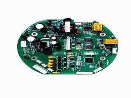
How Are Electronics Circuit Boards Designed?
Once the nets are routed, it’s time to clean up the layout and prepare for manufacturing. This is a semi-additive process, where the layers of the PCB are cleaned up before the copper is deposited on them. The original bare copper on the laminate is first covered with a mask, which exposes those parts of the layer where the copper will be plated. Then, the remaining unmasked area is electroplated with copper to produce plated-through holes, which connect all the conducting layers of the PCB.
The final step is to run a quality control inspection. This is a very important step that ensures the finished circuit board meets its intended specifications, such as ensuring no short circuits or missing components. It also helps catch problems that could have been caused by the imaging or etching processes. This step is also used to check for a proper connection between the component pins and the circuit board, as well as the correct placement of the ICs.
After a thorough visual inspection, the boards are ready for a more detailed mechanical check of their dimensions. They are then shipped to a manufacturer, where they are drilled and etched into their final shapes. The bare circuit boards are then populated with the component leads, which are connected to each other by the conductive vias. This is either done through hole technology, where the component leads are inserted into holes that are surrounded by conductive pads, or surface-mount technology, where the component leads are placed directly on the surface of the board and held in place with solder paste. In some cases, both methods are used in the same board.