Via in Pad Affect the Trace Routing of a PCB
Vias play an important role in the interconnection of layers in PCBs and electronic products. They are used to provide conductive paths between components and facilitate heat dissipation. There are three main types of vias: through hole, blind and buried. Each has its own advantages and disadvantages for use in different applications.
A via in pad is a type of via where the hole for the via is actually on the component pads rather than separate from them. The advantage of this is that it reduces the amount of space required for routing signals between layers. In addition, it eliminates the stub from the discrete via, which improves signal quality.
The downside of this approach is that it requires a more complex fabrication process since the holes for the vias are on the component pads instead of separate from them. This adds to the overall cost of the board, as well as increasing the complexity of the assembly.
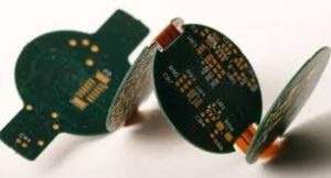
How Does a Via in Pad Affect the Trace Routing of a PCB?
In order to produce a PCB with a via in pad, manufacturers need to utilize specialized drilling equipment capable of producing small-diameter vias and maintaining precise control of the drilling depths. In addition, they must also employ plating techniques to ensure consistent and reliable conductive paths in the vias. They must also take special care to prevent solder paste wicking into the vias during reflow, which can lead to reliability issues. Finally, they must apply rigorous quality control measures to ensure that the resulting PCBs meet industry standards and guidelines.
Depending on the design, a via in pad may be able to decrease the parasitic inductance of a circuit. By eliminating the trace portion of the inductance, this technique can improve signal integrity for high-speed designs and interfaces.
Another benefit of a via in pad is that it allows traces to transition between layers directly beneath components. This can simplify routing paths and potentially allow designers to reduce the number of layers required in a circuit board, which can lower costs.
While it is possible to route a signal through the pad without using a via, this is not recommended since it could result in a short. Instead, it is recommended to use a through-hole via with a minimum annular ring. This will provide the necessary clearance for the traces to pass through and avoid any problems.
Moreover, in order to properly implement a via in pad, it is best to use a separate drill file for the part pads that are to be capped and filled. This will help to avoid confusion on which vias need to be capped and filled. In addition, it will also make it easier to use design rules and cross probing in CAD software to validate that the resulting designs will function correctly. It is also a good idea to consult the manufacturing team to ensure that they are able to implement these features. This will ensure that the resulting PCBs are both functional and cost-effective.